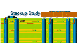
- PCB stack-up design
- Power/ground plane layout design
- Power rail distribution design
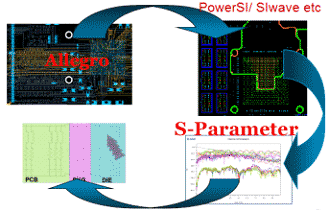
- Power delivery network model extraction
- Simultaneous switching noise analysis and simulation
- Design optimization for power supply to reduce EMI
- Signal quality analysis with power supply noise
- Decoupling scheme and via placement optimization
POWER INTEGRITY
home > services >
power integrity
Power Integrity(PI) Analysis and Simulation
Power integrity (PI) analysis is an essential part of modern electronic design. The ever-increasing numbers of voltages used by ICs, in addition to dramatic increases in power consumption, make the challenges of improving power integrity an exceedingly difficult task. Compounding these challenges are reduced layer counts and finer pitch BGA footprints that perforate copper planes, making it difficult to supply DC voltage and current.
With inadequate power delivery, designs can exhibit seemingly intermittent signal integrity issues, which cause the logic on the board to fail. If power delivery is extremely poor, there can be complete part failure due to inadequate voltage and/or current resulting in a non-functional design.
BestPCB team have extensive experiences in power delivery network design, modeling, analysis and optimization extends to IC, package, and PCB designs in various applications – computing, communications, automobile, medical care, aviation, etc.
Our PI analysis capabilities will ultimately help you reduce prototype spins and get to market faster, while creating more reliable products. BestPCB team can:
- Improve power integrity by identifying power distribution problems early in the design, even prior to layout
- Detect problems with your design that would be difficult to spot in the lab
- Investigate solutions in an easy-to-use what-if environment.
DC Power Analysis
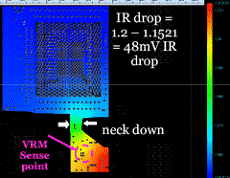
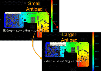
BestPCB team perform pre-layout and post-layout analysis to predict IR drop across PCB board and components to determine optimal PCB plane cu weight (1/2, 1, or 2 oz?) , PCB stackup , power plane shape and via size, number of vias and via location etc.
AC Power Analysis
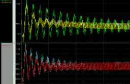
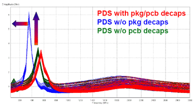
BestPCB team perform pre-layout and post-layout analysis to predict IR drop across PCB board and components to determine optimal PCB plane cu weight (1/2, 1, or 2 oz?) , PCB stackup , power plane shape and via size, number of vias and via location etc.BestPCB team perform pre-layout and post-layout AC power integrity analysis in both frequency domain and time domain to analyze power delivery network (PDN)’s behavior and perform design trade off and optimization to meet system design target.
Typical Power Integrity Analysis Tasks
CONTACT US
Email: [email protected]
(if you have any schematics or notes, please attach them)
Address: 2312 Walsh Ave, Santa Clara, CA 95051, USA
Telephone: (408)868-8018