- Stack-up Analysis & Planning
- Impedance Calculation
- Clock Signal Simulation
- EMI Differential Signal Simulation
- Crosstalk Simulation
- Timing Analysis
- Power Integrity Analysis
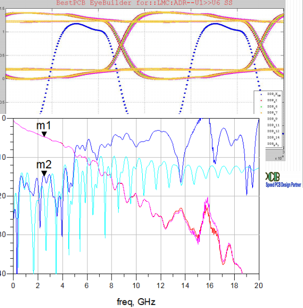
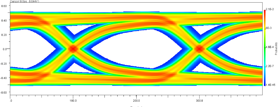
- High Speed Jitter Analysis
- Eye Diagrams Calculation
- Multi-Giga Bit Signaling with 3D Field Solver and Frequency Domain S-Parameter Analysis
SIGNAL INTEGRITY
home > services >
signal integrity
Signal Integrity(SI) Analysis and Simulation
Signal integrity analysis and signal integrity simulation can avoid expensive design re-spins and lengthy time-to-market. BespPCB performs electronic circuit analysis and ensures effective solution results.
Signal integrity(SI) analysis is increasingly important for all types of electronic designs. The placement of chips, wires, and passive components can have a significant impact on the reliability of a product. BestPCB offers signal integrity analysis and signal integrity simulation to circumvent many of the problems which arise unexpectedly with high-speed interconnect. Signal integrity and power integrity analysis can detect problems early in the project design cycle, and thus avoid unexpected design re-spins, thus resulting in shorter time-to-market.
Signal integrity analysis is a highly complex process with a substantial learning curve. BestPCB’s team has the experience and expertise to produce accurate results in a timely fashion. BestPCB can provide assistance with the PCB stack-up definition, as well as execute analyses to prevent crosstalk and reflection issues. Other services include IBIS model generation, performing timing margin analysis reports. BestPCB can also verify the expected behavior and standards conformance of models obtained by suppliers.
BestPCB team have extensive experiences in signal integrity design, modeling, analysis and optimization extends to IC, package, and PCB designs in various applications – computing, communications, automobile, medical care, aviation, etc.
Our SI analysis capabilities will ultimately help you reduce prototype spins and get to market faster, while creating more reliable products.
Typical Signal Integrity Analysis Tasks
CONTACT US
Email: [email protected]
(if you have any schematics or notes, please attach them)
Address: 2312 Walsh Ave, Santa Clara, CA 95051, USA
Telephone: (408)868-8018